| Start | Gleitschirm | Motorrad | Elektronik | Reisen | Seti@Home | Computer | Ratten | Ueber mich | Sitemap | Impressum |
|
Simple but good 2 x 22W Audio Amplifier with LM 1876
LM 1876 made by National Semiconductor is an integrated 2 x 20 Watt hifi audio amplifier. The main difference compared to other amplifier chips in this power class is, that it has very low distortion and noise (THD+N) and a pretty high slew rate. On the other hand, it does not work with a single 12 Volt or 15 Volt power supply, because it is not mainly planed for automotive designs.
On this page, it is shown, how to build a stereo amplifier, using this chip. The complete set of data is available for download, including the schematic, the board layout and description. I have built this amplifier several times and it works very good. I use it for example in my 6 channel amplifier, that is connected to my computer. Four channels are made up of two of this amps and the remaining two channels are made up with a different, more powerful chip, which can also be found elsewhere on this page.
What this circuit provides and what it does not provide:
All features of the chip are supported, such as thermal protection, current limiting, overvoltage and undervoltage protection. The "Mute" and the "Standby" inputs are not used, but are available on a two pin header. They are not usable for left and right channels seperately. Either the whole chip is muted / in standby mode or nothing. There is no volume or sound control. The circuit is not a preamp, but a naked power amp.
The schematic is basically taken from National Semiconductors data sheet for the LM 1876, which can be downloaded here: lm_1876.pdf (322kB) .
Other than the data sheet, my schematic shows both channels. While creating the schematic, I found one thing to be somehow inconsistent with this chip. The chip has individual (per channel) inputs for the positive power supply voltage (Vcc) and for ground (Gnd), but both channels share the same pin for the negative supply voltage (Vee). That does not make too much sense, in my oppinion. I created a test board, where I kept Vcc and Gnd seperate for left and right channel and a second test board, where Vcc and Gnd are shared between the channels. I did not find any differences, that are visible on the oscilloscope or are audible. So I decided to make our life a bit easier and make the schema/layout with shared Vcc/Gnd. Hifi enthusiasts might consider to increase c1 and c2 to 33, 39 or 47 micro Farad. This will improve the low frequency bandwith accuracy. Please see the application section of the data sheet for more information. You will not be able to use my board layout with those bigger caps, because of space limitations.
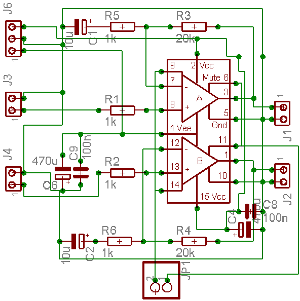
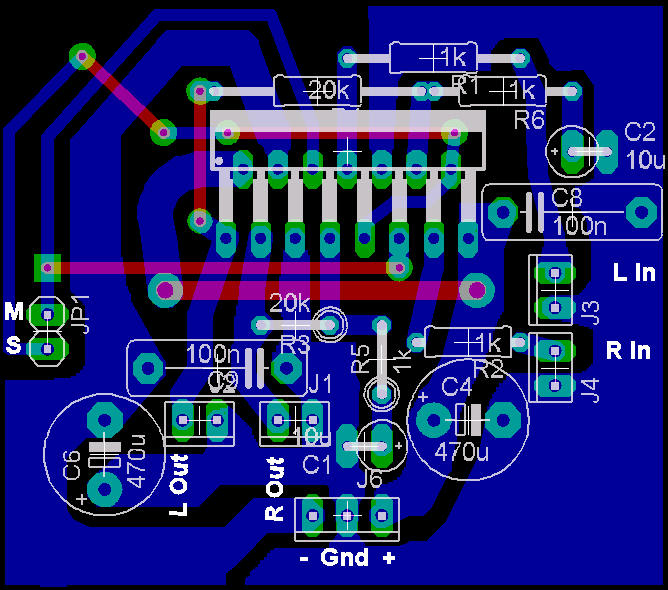
The board layout is very small. Remember, that I designed it for use in a 6 channel amp. I wanted it to be small and handy. The single sided pcb is only appx. 48x 43 mm (1.9x1.65 inches) big. There are some wire bridges shown in red color. Use thick wire for the one in the center of the pcb, because that one carries Vcc. I used two thinner wires and tinned them additionally. Works great.. J3 / J4 are the left /right inputs, J2/J1 the related outputs. The J6 pins are Vee, Gnd and Vcc (left to right). The upper pin of JP1 is "Mute", the other one is "Standby". You do not need to connect them to anywhere. It's just in case you want to use that features sometimes. I have tinned the Output, Power supply and ground traces on the PCB, because they carry higher currents. This layout has two major advantages. It has proven to work and has a very small footprint. But there is no light without shadow.
Here are some of the disadvantages:
All headers are in 2.54 mm (1/10 inch) grid. That is damned ugly small, at least for the power and speaker connections. For the inputs, I soldered two 2-pin headers into the board and then soldered the wires to the pins. For the outputs I drilled bigger holes (1.2 mm or appx 1/20 inch) and soldered the wires to the pcb directly. For the power supply I used a three pin header that I disassembled from an old PC mainboard and the matching three pole connection cable from an old PC cooler fan. The header just fits on the pcb. Those wires really look a little thin, but until now, nothin has started burning and everything works fine. There is "a hell lot of" the pcb behind the 1876 chip. This is not a problem, as long as your heat sink starts a little higher than the pcb. It is an issue, if you want to mount the amp in the middle of a bigger heat sink, as I did it. I had to use an 9 mm "spacer" behind the chip, made from an Aluminium plate. Also some of the solder pads are a little small. You have to be carefull when drilling the holes.
Still want to build this shit ? ;-))
Building the baby is as simple as it looks from the above layout picture.
Download the data package. It contains the PCB layout in different file formats.
To keep the layout simple and nice, I did not try to avoid wire bridges. So there are actually 5 of them on the board. Assemble and solder the parts in the order of their height. Start with the most flat part (wire bridges).
A few words about the power supply. The LM1876 accepts a wide range of suplly voltages. Our circuit is designed for a split power supply. A good choice is anything from +-20V to +-25V. Higher voltages do not bring you any advantages. Lower voltages will decrease the maximum output power. My transformer gives me 2 x 18 Volts. After conversion to DC, the voltage without any load is +-25V. Under heavy load, I still have appx. +-22 V. As I am only using 4 Ohm speakers, this will allways give me maximum power, while the level of heat dissipation is still reasonable. You can find a power supply schematic and layout somewhere else on this page as well.
Testing can be done very easily, with only a multimeter. First of all, connect the inputs to ground. Connect the power supply, but make sure to use 3 Ampere fuses in the power supply unit for testing. If the 3A fuses blow, something is totally wrong. Switch the multimeter to 20V AC voltage and measure the amp outputs. Decrease the voltage display range step by step. You should not find a voltage there. If you don't find an AC voltage, then there is no hum or noise on the outputs with grounded inputs. That's good. Next switch the multimeter to 20V DC voltage and measure the outputs again. Decrease voltage range step by step. There should not be a significant DC voltage on the outputs, as this could toast your speakers. I would say up to 50 Millivolts are OK. Now you could connect some speakers. You should not hear hum or hiss. Next, connect an input source, such as your PCs line out. Make sure to set the output volume in the PC to minimum first. Then slowly increase it and ENJOY ! :-)